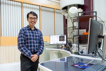
EEE Professor Kim Munho developed a technique to create a higher yield and efficient semiconductors
Scientists from the NTU Singapore and the Korea Institute of Machinery & Materials (KIMM) have developed a technique to create a highly uniform and scalable semiconductor wafer, paving the way to higher chip yield and more cost-efficient semiconductors.
Assistant Professor Kim Munho and his Ph.D. students Kim Youjin and Liao Yikai from the School of Electrical and Electronic Engineering, are part of the NTU-KIMM research team that has come up with this innovative solution.
Semiconductor chips commonly found in smartphones and computers are difficult and complex to make, requiring highly advanced machines and special environments to manufacture.
Their fabrication is typically done on silicon wafers and then diced into the small chips that are used in devices. However, the process is imperfect, and not all chips from the same wafer work or operate as desired. These defective chips are discarded, lowering semiconductor yield while increasing the production cost.
The ability to produce uniform wafers at the desired thickness is the most important factor in ensuring that every chip fabricated on the same wafer performs correctly.
Nanotransfer-based printing– a process that uses a polymer mold to print metal onto a substrate through pressure, or ‘stamping’ – has gained traction in recent years as a promising technology for its simplicity, relative cost-effectiveness, and high throughput. However, the technique uses a chemical adhesive layer, which causes negative effects, such as surface defects and performance degradation when printed at scale, as well as human health hazards. For these reasons, mass adoption of the technology and consequent chip application in devices has been limited.
In their study, which was published in the peer-reviewed journal ACS Nano, the research team from NTU and KIMM reported that their chemical-free printing technique, when combined with metal-assisted chemical etching – a method used to enhance the contrast on surfaces to make nanostructures visible - resulted in semiconductor wafers with nanowires (nanostructures in cylindrical form) that were highly uniform and scalable. The semiconductor also demonstrated better performance when compared with current chips in the market.
Moreover, the fabrication method is also fast and leads to a high chip yield. Prof Kim believes that the technology can scale up into production within the next one to two years. A mutual patent (NTU-KIMM) was already granted in Korea and they have applied for patents in Singapore as well.
There is the opportunity for students to be part of Prof Kim’s research as well. Currently, an MSE student is involved in the research project as part of the Undergraduate Research on Campus (URECA) programme.