Centre of Microsystem Technology

The Microsystem Technologies Development Centre (MTDC) focuses on several key research areas including III-V compound semiconductor growth, device and Integrated Circuit fabrications, Photonics and System-on-Chip Circuit design.
Main Objectives
- To support advanced R&D and build up the indigenous capabilities to meet Singapore’s defence needs in microsystem and related technologies.
- To constantly established joint collaborations with both local and international renowned universities, research institutes and government agencies.
- To work hand-in-hand with Secondary Schools, JC, Polytechnics and the Universities to train students through programmes such as Industrial Attachment, Final Year Project, Young Defence Scientist Programme (YDSP) and Undergraduate Research Experience on Campus (URECA). To date, MTDC has trained many students to provide them with hands-on experience through such programmes.
Find out more information about different areas below:
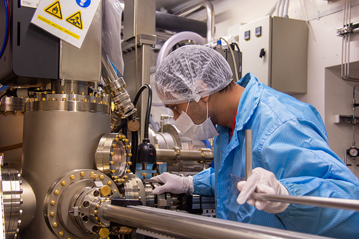 MTDC- GROWTH TEAM
Led By Prof Radhakrishnan K / Dr Dharmarasu Nethaji
This main focus of this team is to develop III-Nitrides epitaxial growth of HEMTs heterostructures on Si and SiC substrates for high power and high frequency applications using Metal Organic Chemical Vapour Deposition (MOCVD) and Molecular Beam Epitaxy (MBE) growth techniques. Recently, this team is also aiming to develop GaN HEMTs on diamond substrate for high power applications. The III-Nitride based novel HEMTs heterostructures such as stress free barrier with better thermal conductivity buffer to enhance device performances and reliability are also being investigated. Other interesting research activities of this team include III-Nitride based intersubband quantum cascade Infrared (IR) and Ultraviolet (UV) detectors, GaN-based Gunn oscillator (self-switching diodes) and GaN HEMTs based gas sensors.
MOCVD and MBE based III-Nitride epitaxial growth capabilities along with non-destructive metrology tools such as high-resolution X-Ray diffraction (HR-XRD), Hall (non-contact), atomic force microscopy (AFM) and bow have been established. These epigrowth facilities are ISO 9001:2015 certified. AlGaN/ GaN HEMTs growth processes on 4 inch Si and SiC substrates with excellent properties for 0.25μm gate technology have been achieved. Key challenges in the growth of GaN HEMTs heterostructures have been overcome, such as stress mitigation layer for crack-free wafer, low buffer leakage current and high breakdown voltage. The GaN HEMTs growth process repeatability has been achieved with in-wafer and wafer-to-wafer 2DEG variation not more than 10%. The device performances show low RF loss with the state-of-the-art output power density. Other important achievements include realization of GaN-based mid-infrared and UV detectors, and gas sensors.

MTDC- Fabrication Team
Led By Prof Ng Geok Ing / Dr Subramaniam Arulkumaran
The vision of MTDC is to be a leading research centre providing cutting-edge Monolithic Microwave Integrated Circuits (MMIC) and related technologies that will enhance Singapore’s defence capabilities. This platform will also enable Future Systems and Technology Directorate (FSTD) to generate intellectual property (IP) and know-hows through advanced R&D on key technologies to support the future defence needs of Singapore.
- Development of gallium nitride (GaN) high-electron-mobility transistor (HEMT) and MMICs,
- Advanced Ceramic Thin Film Filters,
- Diamond-on-GaN,
- GaN-on-Diamond,
- Q-Bits for Quantum Computing,
- and Photonic Chip Fabrication.
The team has achieved the following:
- Certified with International Organization for Standardization (ISO) 9001: 2015 for “manufacture of semiconductor wafers and passive components on ceramic substrates”
- 0.25um gate GaN-on-SiC HEMT technology and performance of MTDC Developed photonic chips (LN MIOC) is comparable to that of external foundry
- GaN HEMTs, Resistor and Capacitors are passed all process qualification tests up to the level of Very High Altitude

Photonics
Led By Dr Liu Chongyang
This programme currently has two areas of focus, photonics subsystem and optoelectronic devices. The team aims to indigenously develop photonic subsystems, integrated optoelectronic devices that will be
of interest to Future Systems & Technology Directorate/ Defence Science Organisation (FSTD/ DSO), and to produce them in small quantities sufficient for testing and evaluation.
Photonics
subsystem: The efforts in this field focuses on the development of sub-systems that utilise photonics to perform microwave signal processing, as well as components that can be used in the various fibre-based
photonic architectures.
Optoelectronic devices: We seek to develop and prototype photonic devices and components that inter-convert optical and electrical energy, such as ultrafast laser diodes,
high power laser diodes for pumping fiber lasers, as well as photodiodes with customised specifications.
In addition, the team is also working on building devices and modules on silicon photonics,
III-V compound semiconductors, lithium niobate and many other electro-optic material platforms that allow electrical and optical signals to interface with each other, such as switches, modulators and
oscillators/ resonators.
Our research activities in photonics are supported by state-of-the-art nano-fabrication facilities (N2FC) which comprises of class 100 cleanroom (CR1) and class
10/100 cleanroom (CR2) in the school of Electrical & Electronic Engineering (EEE, NTU). The team also works closely with the MTDC team for device fabrication due to the compatibility with the commonly
known semiconductor fabrication processes.
Till now, the following selected achievements has been obtained by the team.
Ultrafast mode-locked laser diode up to 40GHz;
High
speed (> 40GHz) and high power RF Uni-Traveling-Carrier Photodiodes (UTC-PDs);
High power laser diode up to 50W;
Lithium Niobate modulators up to 20GHz and Lithium Niobate photonic chips;
High Q (> 5 x 10⁶) whispering gallery mode disk based on Lithium Niobate and Lithium Tantalate;
Fiber-based Opto-electronic oscillator (OEO) with low phase noise at x-band.
Circuit Design System on Chip
Led By Prof Joseph Chang
The mission of the Circuit Design SoC team is to provide Singapore’s Defence with innovative cutting-edge electronic solutions in the form of System-on-Chip (SoC) to meet Defence’s short-term needs, and to explore emerging technologies to support Defence’s long-term needs. The research and engineering scope includes sophisticated and very-high reliable SoCs, such as ultra-high-speed integrated circuits, high-speed wideband data converters, radiation-hardening-by-design integrated circuits, ultra-low-power digital circuits and low-power ultra-high-accuracy analog readout circuits for sensors. In our research, the team continuously pursue architectural and circuitry innovations to enhance the SoC performance in all aspects that are beyond the state of the art, and on the basis of engineering science. The outcome of our research significantly enhances the capabilities of Singapore’s Defense, with innovative enabling technologies.