TEM cluster: Applications & Instruments
Transmission electron microscopy (TEM) is a powerful characterisation technique that provides imaging, diffraction, spectroscopy and advanced analytical capabilities, enabling structural, crystallographic, elemental, chemical and functional characterisation across multiple length scales. It plays a vital role in research and innovation across materials science, nanotechnology, semiconductors, energy, catalysis, pharmaceuticals and the life sciences.
Imaging can be performed in both conventional transmission electron microscopy (TEM) and scanning transmission electron microscopy (STEM) modes. Complementary techniques—including energy-dispersive X-ray spectroscopy (EDS), electron energy loss spectroscopy (EELS), electron diffraction, electron tomography, electron holography, differential phase contrast (DPC), four-dimensional STEM (4D STEM) and Micro Electron Diffraction (MicroED)—provide comprehensive insights into the structure, composition and properties of materials.
The FACTS TEM Cluster currently comprises five field-emission transmission electron microscopes (TEMs), including two aberration-corrected TEMs, providing researchers with a comprehensive suite of advanced electron microscopy capabilities.
FACTS has five field-emission transmission electron microscopes (TEMs) that support both conventional transmission electron microscopy (TEM) and scanning transmission electron microscopy (STEM).
In conventional TEM mode, a thin specimen is illuminated by an electron beam. The transmitted and diffracted electrons are used to generate high-resolution images and diffraction patterns, enabling the investigation of specimen morphology, microstructure and crystal structure.
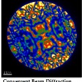
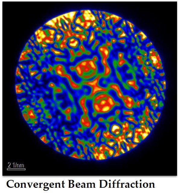
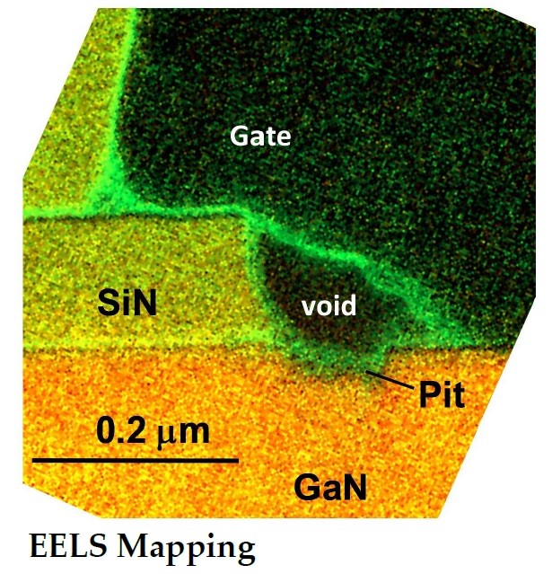
The microscopes are also equipped for scanning transmission electron microscopy (STEM), in which a focused electron probe is scanned across the specimen. This enables high-resolution imaging together with analytical techniques such as energy-dispersive X-ray spectroscopy (EDS), electron energy loss spectroscopy (EELS) and convergent beam electron diffraction (CBED), providing complementary structural, crystallographic, elemental and chemical information from the regions of interest.
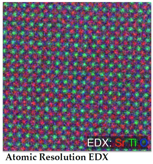
Aberration-corrected transmission electron microscopes (ACTEMs) are designed to achieve atomic-resolution imaging by correcting lens aberrations that limit the spatial resolution of conventional TEMs. They enable direct visualisation of atomic structures and provide advanced imaging and analytical capabilities for investigating the structure, chemistry and functionality of materials at the atomic scale.
The FACTS TEM Cluster houses two aberration-corrected TEMs, operating at accelerating voltages of 300 kV and 200 kV.
The JEOL Grand ARM300F (300 kV) is equipped with both an image corrector for TEM mode and a probe corrector for STEM mode. It is fitted with a large-area energy-dispersive X-ray spectroscopy (EDS) detector and an electron energy loss spectrometer (EELS), supporting atomic-resolution imaging and advanced analytical characterisation. In addition, it supports specialised techniques including electron tomography and electron holography.
The JEOL ARM200F (200 kV) operates in STEM mode with a probe corrector and is equipped with dual large-area energy-dispersive X-ray spectroscopy (EDS) detectors plus EELS, enabling high-sensitivity elemental mapping and high-resolution analytical STEM.
Both aberration-corrected TEMs support four-dimensional scanning transmission electron microscopy (4D STEM), enabling simultaneous analysis of crystallography, crystal orientation, strain, phase, and electric and magnetic fields from a single experiment.
Both ACTEMs are equipped with a high-speed Gatan OneView™ 4k × 4k CMOS camera, enabling rapid image acquisition and supporting a wide range of in situ experiments.
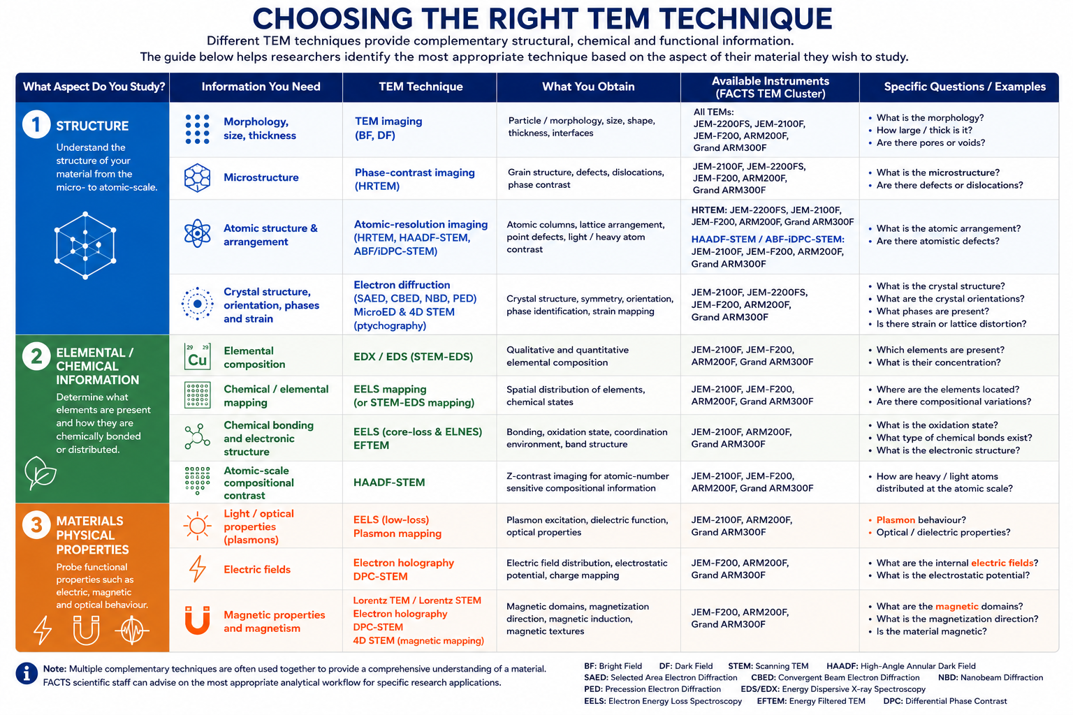
The FACTS TEM Cluster supports a comprehensive suite of imaging, diffraction, spectroscopy and advanced analytical techniques for investigating the structure, chemistry and functionality of materials across multiple length scales. The following techniques are available to address a wide range of research questions.
Imaging
Transmission Electron Microscopy (TEM) Mode
The most common TEM imaging mode, where a broad, stationary, parallel electron beam illuminates the specimen. Bright-field, dark-field and high-resolution imaging are commonly performed in this mode.
Scanning Transmission Electron Microscopy (STEM) Mode
A focused electron probe is scanned across the specimen to generate high-resolution images and analytical signals. STEM forms the basis for techniques such as HAADF imaging, EDS, EELS, DPC and 4D STEM.
Bright-Field TEM (BF-TEM)
Provides high-resolution images of specimen morphology, grain structure, interfaces and crystal defects using transmitted electrons.
Dark-Field TEM (DF-TEM)
Uses diffracted electrons to selectively highlight specific crystal orientations, phases and defects, making it particularly useful for microstructural and crystallographic studies.
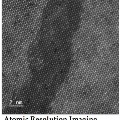
High-Resolution TEM (HRTEM)
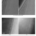
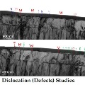
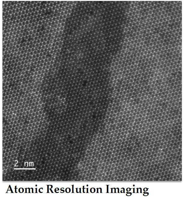
Reveals atomic arrangements and crystal lattices through phase-contrast imaging, enabling direct investigation of interfaces, defects and nanoscale structures.
High-Angle Annular Dark-Field STEM (HAADF-STEM)
Produces atomic-number (Z-contrast) images using electrons scattered through high angles, allowing direct visualisation of heavy atomic columns.
High-Resolution STEM
Employs a finely focused electron probe to directly image and analyse individual atomic columns within crystalline materials.
Diffraction
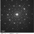
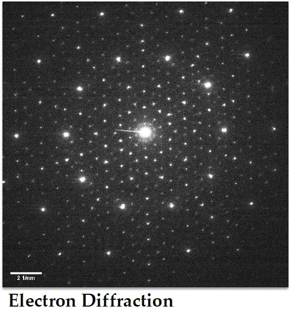
Electron Diffraction
Determines crystal structure, phase, orientation, symmetry and lattice parameters from nanoscale volumes with high spatial resolution.
Micro Electron Diffraction (MicroED)
Determines the atomic structure of extremely small crystals that are unsuitable for conventional single-crystal X-ray diffraction, making it particularly valuable for pharmaceuticals, nanocrystals and beam-sensitive materials.
Spectroscopy
Energy-Dispersive X-ray Spectroscopy (EDS)
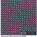
Uses characteristic X-rays generated by electron–matter interactions to determine elemental composition and perform elemental mapping in STEM mode.
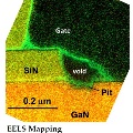
Electron Energy Loss Spectroscopy (EELS)
Measures the energy lost by transmitted electrons to reveal elemental composition, chemical bonding, oxidation state and electronic structure with nanometre- to atomic-scale resolution.
Energy-Filtered Transmission Electron Microscopy (EFTEM)
Uses energy-filtered electrons to generate elemental, chemical and thickness maps over relatively large fields of view, complementing STEM-EELS analysis.
Advanced Techniques
Differential Phase Contrast (DPC)A STEM imaging technique that quantitatively maps internal electric and magnetic fields, providing insights into the functional behaviour of advanced materials.
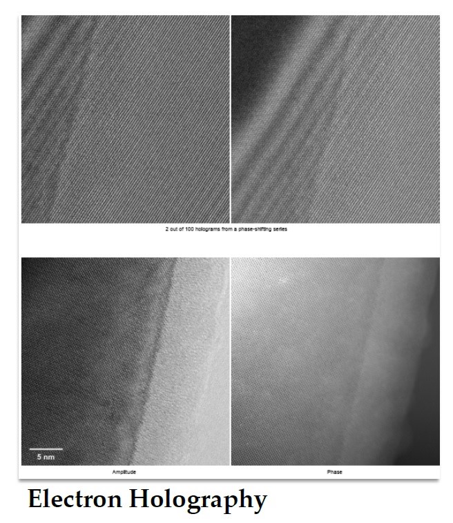
Electron Holography
Reconstructs the phase of the electron wave to quantitatively measure electrostatic potentials and magnetic induction with exceptional sensitivity and spatial resolution.
Electron Tomography
Reconstructs a three-dimensional representation of a specimen from a series of tilted TEM or STEM images, revealing nanoscale morphology, internal architecture and structural connectivity.
Four-Dimensional Scanning Transmission Electron Microscopy (4D STEM)
Records a complete electron diffraction pattern at every probe position, enabling simultaneous analysis of crystallography, strain, phase, electric and magnetic fields, and quantitative phase imaging from a single experiment.
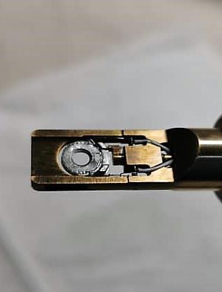
In situ TEM enables specimens to be observed under controlled experimental conditions during imaging, allowing researchers to directly investigate structural and functional changes in real time. The FACTS TEM Cluster supports a range of in situ experiments, including heating, cooling, electrical biasing, and liquid-cell studies, using specialised TEM sample holders.
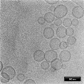
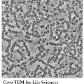
Cryo-TEM can be performed using dedicated cryogenic sample holders that maintain specimens at cryogenic temperatures during imaging. This enables beam-sensitive and soft materials to be examined using lower electron doses, thereby minimising electron beam damage while preserving their native structure.
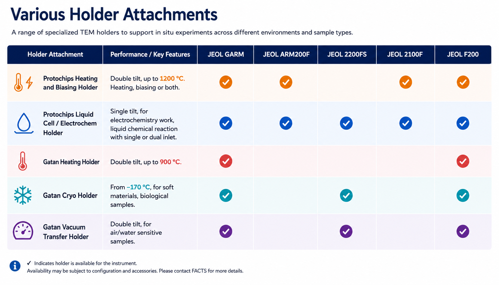
To support advanced electron microscopy applications, the FACTS TEM Cluster provides a range of specialised TEM specimen holders for in situ heating, electrical biasing, electrochemistry, cryogenic imaging, and air-sensitive sample transfer. The availability of each holder varies by instrument and is summarised below.
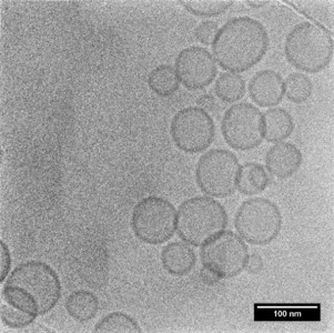
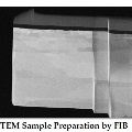
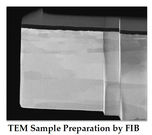
Sample preparation involves preparing the sample to be analysed into a thin cross-section, which can then be placed in the electron beam illumination path. For colloidal samples, this can be drop casting on a copper grid and drying. Bulk samples can be either prepared as a small thin section by mechanical means, or by ion milling methods such as using the Focused Ion Beam (FIB).
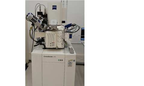
FACTS has a FIB for TEM lamellae preparation. The FIB is a versatile analytical tool for materials science, semiconductor industry, etc. It is built on a FESEM platform for site-specific analysis, cross-sectioning, deposition and removal of materials, TEM lamella preparation etc. The FIB is equipped with a Ga ion beam, Pt and C gas injection systems and an in-situ manipulator for lamella preparation and nanofabrication work.
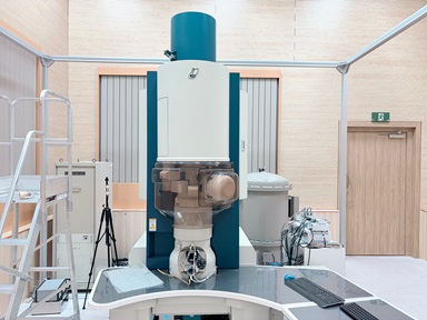
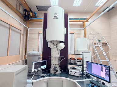

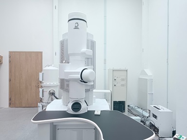
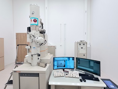
AToMs is one of the largest advanced TEM facilities in Asia housing 8 TEMs from FACTS and NISB. Our high-end instruments include aberration-corrected TEMs (AC-TEMs) dedicated to materials characterisation at the atomic level and cryo-TEMs for 3D reconstruction of biomolecules.
The coexistence of microscopy techniques for both physical and life sciences within AToM will bring forth multidisciplinary expertise and stimulate interaction between these dynamic research areas.
The TEMs are housed in specially designed low-noise and low-vibration rooms with stable temperature and magnetic shielding.
AToM was officially opened on the 11th Jan 2019.