Cleanroom 2

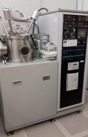
A sputtering system which is equipped with two cathodes-one 600W RF and one 600W DC for deposition of metals and dielectrics. The chamber is pumped by a turbo pump. Single or co-sputter is possible.

A locally designed sputtering system which is equipped with three cathodes-one 600W RF and two 1500W DC. The chamber is pumped by a turbo pump. Single or co-sputter is possible.

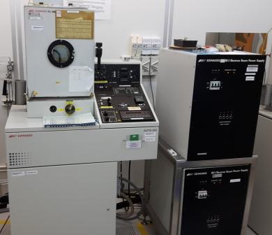
The Auto306 is a compact, versatile vacuum coater used for deposition of metals. It comprises of a 3kW E-Beam gun, a 4-pocket turret which enables users to insert 4 x 4cc crucibles of different target materials.
Remarks: Deposition of Fe is not allowed.

The Auto306 is a compact, versatile vacuum coater used for deposition of metals. It comprises of a 3kW E-Beam gun, a 4-pocket turret which enables users to insert 4 x 4cc crucibles of different target materials.
Remarks: Deposition of Fe is not allowed.

The Auto306 is a compact, versatile vacuum coater used for deposition of metals. It comprises of a 3kW E-Beam gun, a 4-pocket turret which enables users to insert 4 x 4cc crucibles of different target materials.
Remarks: Deposition of Fe is not allowed.

This system is used for InP & GaAs-based heterostructure growth. The source materials are transported by way of a carrier gas and gradually supplied to the reactor.

A dual chamber system capable of deposition and etching of 6“or smaller wafers. The right chamber is for Plasma Enhanced Chemical Vapor Deposition (PECVD) while the left chamber is for Reactive Ion Etching (RIE).
Material Deposition/Etching.: Dedicated for SiN and SiO2
Gases available: SiH4, NH3, N2O, O2, CF4 and N2
Small pieces up to 6" in diameter.

A single chamber system capable of deposition and etching of 6“or smaller wafers. It is equipped with a loadlock with robot handling for transfer of wafer.
Gases available: SiH4, SF6, CHF3, C4F8, Ar, O2, CF4 and N2

This system is designed for nanowire growths for Si Nanowire and GaN Nanowire.

A Rapid Thermal Processing (RTP) system consisting of a single high temperature rapid annealing chamber.

CRIE-200 plasma etching system is designed for III-V compound semiconductor etching. The system comes with a loadlock and is connected to Cl2, BCl3, CH4 and O2.

CLEN-100 Plasma stripping system for tough jobs as well gentler applications such as descumming and removing organics.

UV radiation, ozone and heat to gently remove organic materials for a variety of substrates.

The Vistec EBPG5200 is a high performance nanolithography system with full 200mm writing capability. This Electron Beam Lithography system offers a wider range of solutions for both direct write nano-lithography and R&D mask making.
Main Field Beam deflection: 20 bit DAC
Field size: 168 μm x 168 μm to 1 mm x 1 mm (at 20, 50, 100 kV)
Min. theoretical spot size: 2.2 nm
Stage Travel range: 210 mm ×210 mm
Writing Mode: Step & Repeat
Automation: 10 position airlock
Thermal stability: < 50 nm / hr (open loop)
Footprint: < 20 m²
Minimum feature size: < 8.0 nm
Stitching and overlay accuracy: < ±12 nm

The MJB4 is equipped with a 350W mercury lamp providing UV Exposure wavelengths of 350–450nm. The machine is equipped with High Precision Alignment stage and microscope manipulator.
Substrate size: Up to 4” Diameter
Mask: 5”
UV Range: 405nm, 320nm


Bench 1 - Comes with ultrasonic function
Bench 2 - Comes with hot plate function (limit top 2 hours)

Wet etching and acid cleaning with DI water rinsing.

Wet etching and acid cleaning with DI water rinsing.

A Field Emission Scanning Electron Microscope (FESEM) system

The Dimension Edge Atomic Force Microscope (AFM) incorporates Bruker’s PeakForce Tapping technology. The system has an X-Y Scan range of 100 μm x 100 μm. This unit is provided with Contact Mode and Tapping Mode AFM. The raw data is captured by the independent Nano Drive software and the images are post processed using NanoScope Analysis software.

A variable angle spectroscopic ellipsometer for the measurement of thickness, refractive index(n) and absorption index(k) of thin film.
A variable angle spectroscopic ellipsometer for the measurement of thickness, refractive index(n) and absorption index(k) of thin film.

The X'Pert³ MRD XL meets all the high-resolution XRD analysis requirements of the semiconductors, thin films, and advanced materials industries. Complete wafer mapping up to 200 mm is possible. The X’Pert3 version comes with longest lifetime of incident beam components (CRISP) and maximum uptime with pneumatic shutters and beam attenuators.
