Equipment

Evatec Clusterline CLC200 Sputterer
Location: S1-B5a-01 (Cleanroom 1)

Cello Ohmiker-60BL e-beam evaporator
Location: S1-B5a-01 (Cleanroom 1)
Users would need to provide material and crucibles not available in N2FC

Cambridge Nanotech ALD Location
Location: S1-B5a-01 (Cleanroom 1)

P5000 Applied Materials PECVD Location
Location: S1-B5a-01 (Cleanroom 1)

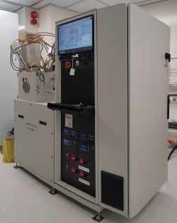
Cello Aegis-20 PECVD Location
Location: S1-B5a-01 (Cleanroom 1)

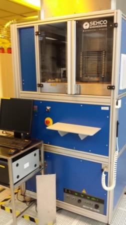
SEMCO PECVD Location
Location: S1-B5a-01 (Cleanroom 1)

Denton Explorer 18 Sputter System
Location: S1-B5a-01 (Cleanroom 1)
The Denton Explorer 18 Sputter System is configured with three 3-inch cathodes and is equipped with two 600W RF generators and two 1200W DC power supplies. Designed for sputter down configuration, each cathode can be selected for RF or DC sputtering via software switching.
The front-loading chamber is pumped by a turbo pump. A 6” rotating stage is incorporated for better uniformity and can accommodate small samples and wafers up to 6" in diameter.
Users would need to provide targets not available in N2FC

Elite Sputter Location
Location: S1-B5a-01 (Cleanroom 1)
Users would need to provide targets not available in N2FC

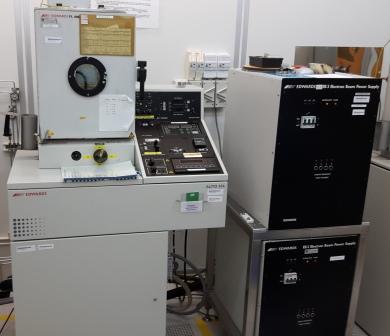
Edwards Auto306 E-Beam Evaporator #1
Location: S1-B5a-01 (Cleanroom 1)
Remarks: Deposition of Fe is not allowed.

Edwards Auto306 E-Beam Evaporator #2
Location: S1-B5a-01 (Cleanroom 1)
Remarks: Deposition of Fe is not allowed.

HHV Auto306 E-Beam Evaporator #3
Location: S2.2-B5-01a
(Cleanroom 2)
Remarks: Deposition of Fe is not allowed.

SEMCO LPCVD
Location: S2.2-B5-01a (Cleanroom 2)
Small pieces up to 2" in diameter

AS-One RTP
Location: S1-B5a-01 (Cleanroom 1)
A Rapid Thermal Processing (RTP) system consisting of a single high temperature rapid annealing chamber.

SEMCO JIPELEC RTP
Location: S1-B5a-01 (Cleanroom 1)
A Rapid Thermal Processing (RTP) system consisting of a single high temperature rapid annealing chamber.
Remarks: Non-Metal compatible.

Varian EHP-220 Ion Implanter
Location: S1-B5a-01 (Cleanroom 1)
An Ion Implantation system equipped with robot handling tool.

MRL Oxidation Furnace B3, MRL Alloy Furnace B4
Location: S1-B5a-01 (Cleanroom 1)
For thermal oxidation process.
MRL Alloy Furnace B4
For thermal process with N2 or O2 or H2 gases. Maximum temperature up to 950°C. Wafer/sample size ranges from small sample up to 6” round Si wafer.
Remarks: Metal compatible (For B3 & B4 only)

Oxford PlasmaPro100 ICP-RIE
Location: S1-B5a-01 (Cleanroom 1)
An Inductive Coupled Plasma Reactive Ion Etching (ICP-RIE) system consisting of 1 etch chamber and 1 loadlock chamber equipped with robot handling tool.
Remarks: Non-Metal compatible

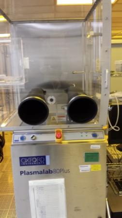
Oxford Plasmalab80 RIE
Location: S1-B5a-01 (Cleanroom 1)
A Reactive Ion Etching (RIE) system consisting of 1 etch chamber and 1 glovebox enclosure.
Remarks: Metal compatible

Oxford Estrelas Deep Si-RIE
Location: S1-B5a-01 (Cleanroom 1)
A Deep Silicon Reactive Ion Etching (DSRIE) system (BOSCH process) consisting of 1 etch chamber and 1 loadlock chamber equipped with robot handling tool.
Remarks: Non-Metal compatible
Sidewall angle: 90±1o
Scallop size: <30nm

AV RIE
Location: S1-B5a-01 (Cleanroom 1)
A Reactive Ion Etching (RIE) system consisting of 1 etch chamber.
Remarks: Non-Metal compatible

AST CRIE-200 Reactive Ion Etcher
Location: S1-B5a-01 (Cleanroom 1)

AST CLEN-100 Descum
Location: S1-B5a-01 (Cleanroom 1)

SAMCO UV Ozone Dry Stripper
Location: S2.2-B5-01a
(Cleanroom 2)

Tepla O2 Plasma Asher
Location: S1-B5a-01 (Cleanroom 1)
An Oxygen Plasma Photoresist Stripper system consisting of 1 chamber to remove bulk photoresist using O2 microwave plasma without causing damage to the surface.

UVO system
Location: S1-B5a-01 (Cleanroom 1)
A Ultra-Violet Ozone (UVO) Cleaner system consisting of 1 compartment for the surface cleaning using UV rays & Ozone without causing damage to the surface.
Remarks: Metal compatible

DWL-200 Mask Writer
Location: S1-B5a-01 (Cleanroom 1)
A Mask writer system is used for writing mask with laser.

Suss Microtec Developer
Location: S1-B5a-01 (Cleanroom 1)
A PR Developer system is used for photoresist development purpose.

Suss MicroTec PR Coater
Location: S1-B5a-01 (Cleanroom 1)
A Spin Coater system is used for photoresist coating purpose.

Suss MircoTec MABA8Gen4 Mask Aligner System
Location: S1-B5a-01 (Cleanroom 1)
LED Lamp for exposure of photoresist (PR). Wafer sizes are only restricted to 2x2cm square sample, 4”, 6” and 8” round Si wafer.
A Mask Aligner system is used for photoresist pattern alignment with LED exposure purpose.

Karl Suss MJB 4 Mask Aligner #1 & #2
Location: S1-B5a-01 (Cleanroom 1)
Substrate size: Up to 4” Diameter
Mask: 4" or 5”
UV Range: 405nm, 320nm

Vistec E-Beam Lithography
Location: S2.2-B5-01a
(Cleanroom 2)
Main Field Beam deflection: 20 bit DAC
Field size: 168 μm x 168 μm to 1 mm x 1 mm (at 20, 50, 100 kV)
Min. theoretical spot size: 2.2 nm
Stage Travel range: 210 mm ×210 mm
Writing Mode: Step & Repeat
Automation: 10 position airlock
Thermal stability: < 50 nm / hr (open loop)
Footprint: < 20 m²
Minimum feature size: < 8.0 nm
Stitching and overlay accuracy: < ±12 nm

YES HMDS Priming Oven
Location: S1-B5a-01 (Cleanroom 1)
A Priming Oven system is used for HMDS priming before PR coating.

CDE ResMap Rs four point probe measurement
Location: S1-B5a-01 (Cleanroom 1)
An automatic Rs (sheet resistivity) mapping system. Wafer size ranges from 4” up to 8” round Si wafer.
An Automatic Rs (sheet resistivity) mapping system is used for the film sheet resistivity measurement using four point probe.

Bruker Dektak XT Step Profiler
Location: S1-B5a-01 (Cleanroom 1)
It is used for Step height measurement for film profile.

Filmetrics Film Thickness Measurement
Location: S1-B5a-01 (Cleanroom 1)
Ordinary light. Wavelength 400-1000nm, Beam size 6mm

Keyence VHX-7000 Digital Microscope
Location: S1-B5a-01 (Cleanroom 1)
Digital Microscope equipped free-angle stand motorized Z&XY stage and 20X to 6000X magnification high-resolution lens.
Digital Microscope equipped free-angle stand motorized Z&XY stage and 20X to 6000X magnification high-resolution lens. Fully auto control system. Multi lighting and observation functions.

Apreo-S FESEM
Location: S2.2-B5-01a
(Research Room)

Bruker Dimension Edge Atomic Force Microscope
Location: S1-B5a-01 (Cleanroom 1)

J.A.Woolam Spectroscopic Ellipsometer
Location: S2.2-B5-01a
(Research Room)

X’Pert3 MRD (XL) X-Ray Diffractometer
Location: S2.2-B6-01
(Cleanroom 2 Subfab)

Verteq Megasonic Cleaner
Location: S1-B5a-01 (Cleanroom 1)
A Megasonic Cleaner system consisting of 2 compartments including megasonic and quick dump rinse (QDR) for the surface cleaning.

Orbis Chemical Mechanical Polishing (CMP)
Location: S1-B5a-01 (Cleanroom 1)
A CMP system consisting of 2 rotating platens (catered for 4”, 6” and 8” wafer substrate).
Remarks: Metal compatible
Material to be polished: SiO2

Apet IPA Dryer
Location: S1-B5a-01 (Cleanroom 1)
An IPA Dryer system is used for wafer drying purpose.
Remarks: Non-Metal compatible

Verteq SRD-MK2
Location: S1-B5a-01 (Cleanroom 1)
A Spin Rinse Dryer (SRD) system is used for wafer drying purpose.

GTX WB-MK-2 Wet Bench (HF)
Location: S1-B5a-01 (Cleanroom 1)
A Wet Bench system is used for the removal (wet etching) of Silicon Dioxide on small piece of wafer with diluted HF purpose.

GTX WB-PC-1 Wet Bench
Location: S1-B5a-01 (Cleanroom 1)
A Wet Bench system is used for the Piranha cleaning purpose.
Remarks: Non-Metal compatible

Solvent Wet Bench
Location: S1-B5a-01 (Cleanroom 1)
Bench 1 - Comes with ultrasonic function
Bench 2 - Comes with hot plate function (limit top 2 hours)

Acid Bench
Location: S1-B5a-01 (Cleanroom 1)

ADT 7120 Dicing Saw
Location: S1-B5a-01 (Cleanroom 1)
A wafer dicing system is used to cut the wafer into small dies.

K&S Wire Bonder Model 4524
Location: S1-B5a-01 (Cleanroom 1)
A wire bonder system is using Gold Wire bonding for dies.
