Accelerating Design-to-Layout Photonics-Integrated Ion-Trap for Quantum Computing
Synopsis
This technology introduces an AI-assisted platform that streamlines the design of photonics-integrated ion trap systems for quantum computing. By automating simulation, verification, and layout generation, it reduces technical barriers, accelerates turnaround time, and minimises resource use.
Opportunity
With the increasing demand for higher computational power, quantum computing has received growing attention due to its ability to perform parallel processing. Among the different approaches, ion trap quantum computing stands out as a promising option. Unlike other methods, such as superconducting qubits, ion trap systems can operate at room temperature and are compatible with standard semiconductor manufacturing processes. However, there is currently no standardised process design kit (PDK) available for developing photonic circuits in ion trap systems, resulting in the in-depth technical expertise needed to handle the complex design and optimisation process of photonic devices.
The technology owner has leveraged on their patent pending photonic design process to develop an AI-assisted platform to assist and accelerate the design-to-layout process of photonics-integrated ion trap systems. By specifying the desired parameters, such as trapped ion species, photonic components and ion trap, users can automatically validate via simulation and generate a Graphic Data System (GDS) layout that is ready-to-fabricate while meeting the photonic design requirements. This results in increased productivity by reducing guesswork and resources, reducing verification turnaround time and lowering the technical barrier required within the design process.
The technology owner has successfully conducted a pilot test with a Singapore-based company in developing a photonic chip utilising their platform. Currently, the owner is actively seeking industrial collaborators interested in exploring photonic applications in quantum computing device design and manufacturing.
Technology
The technology solution leverages on the technology owner’s technical research and expertise on on-chip ion trap development to develop the AI-assisted digital platform catered to accelerate the design process of such photonics-integrated ion trap system. The key features include:
- Input parameters such as intended photonic wavelength (from visible to infrared), trapped ion species, photonic components
- Automated design of 4 gratings for trapping ability of ion-trap
- Technical processing of numerous design and considerations, such as broadband grating couplers for input-coupling of light, output grating of couplers and ring resonators for the filtering of wavelengths and respective light sources pairing
- Built-in formation and performance verification of constructed photonics circuit into on-chip ion trap
- Automated generation of photonic circuit in a ready-to-tape-out DGS format layout
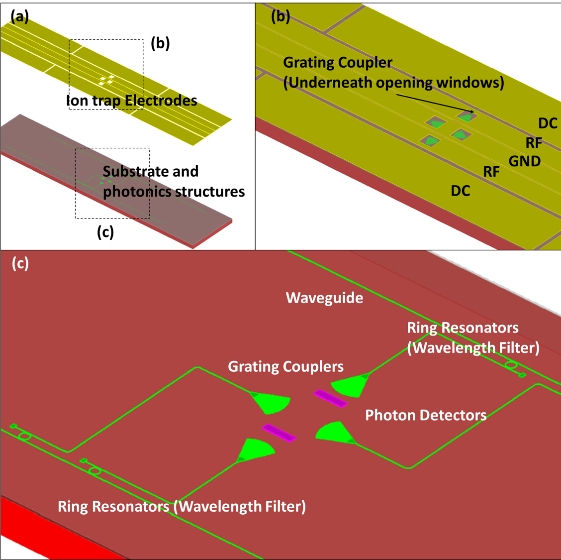
Figure 1: Schematics of a photonics--integrated ion trap.
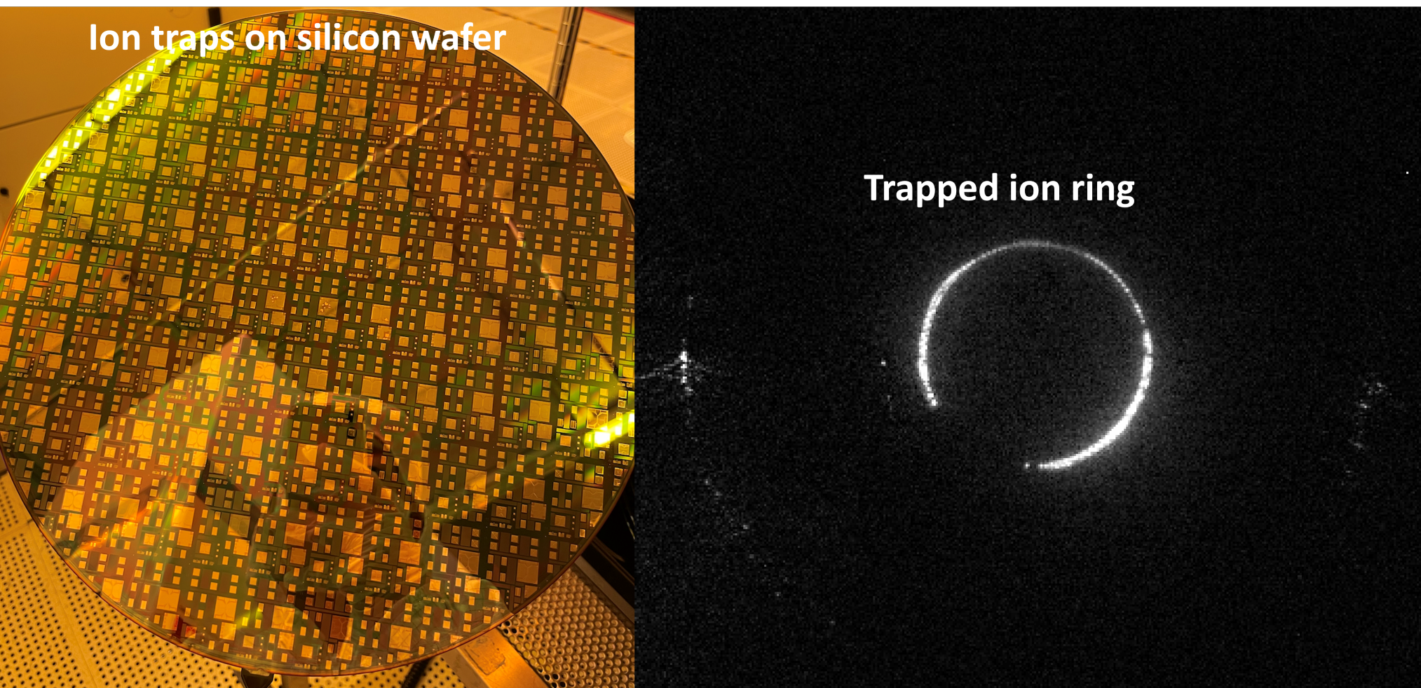
Figure 2: Corresponding image of the photonics--integrated ion trap.
Applications & Advantages
Given the technology solution being utilised within the ion-trap design and fabrication process, below are some potential applications in which have the capability to leverage on the solution, including:
- Quantum computing companies leveraging on the ion-trap system for its working mechanism
- Photonic integrated circuits (PICs) and co-packaged optics (CPO) who requires stringent production of photons
- Quantum clock applications requiring strict ion-trap focusing on optical transitions.
- Industrial players within the photonics industry looking to accelerate their verification turnaround time
This AI-assisted platform solution can automatically internalise the in-depth technical knowledge required to design photonic devices needed for ion trap systems, integrate them into the ion trap layout, and generate a tape-out-ready design. It has the potential to significantly reduce the time, manpower and technical resources required in the traditional chip design process, particularly in the development of photonics-integrated ion trap systems.
.tmb-listing.jpg?Culture=en&sfvrsn=57e7d9a3_1)


.tmb-listing.jpg?Culture=en&sfvrsn=3b74ec1c_1)