
Scalable Production of Low-Defect TMD Monolayers
04 Jul 2024
10.00 AM - 11.00 PM
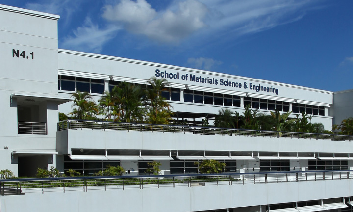
MSE E-Learning Studio (N4.1-B2-02)
Alumni, Current Students
NTU MSE Seminar Hosted by Professor Alex Yan Qingyu
Abstract
One of the key challenges in utilizing two-dimensional (2D) semiconducting transition metal dichalcogenides (TMDs) for industrial applications is achieving large-scale growth with continuous single crystallinity, low defect density, and spatial homogeneity. Here, we present our recent advancements in growing TMD monolayers with single orientation on 2-inch sapphire substrates and our hydroxide-assisted method for achieving low-defect-density growth of these monolayers.
To achieve large-area and grain boundary-free growth of 2D materials, it is critical to understand the fundamentals of the substrate-2D interaction to enable the mono-orientation of these 2D domains. Taking a few examples including 2D TMD, hBN, and perovskites, we would like to discuss the factors that control epitaxy. Detailed analysis will be provided to illustrate the following points. (1) In the situation that 2D seeds strongly bind to the atomic substrates edges, seed nucleation and orientation are controlled by the step edges. (2) In the circumstance that 2D seeds do not strongly bind to the step edges, the epitaxy of 2D is governed by the atomic structures (and symmetry) of the substrates. Hence, the reconstruction of the surfaces of substrates to only a single type (symmetry) is necessary for the single-crystal epitaxy of monolayer TMDs without the aid of step edges. (3) Precursors may react with the substrate surfaces to change the substrate atomic structures and thus the orientation of 2D materials. For example, the surface sulfurization of sapphire drastically changes the orientation preference.
Although single-crystal TMD monolayers achieved via chemical vapor deposition (CVD) exhibit homogeneous electrical performance due to reduced grain boundaries, the electrical quality is still limited by abundant point defects such as vacancies and impurities introduced during synthesis. We report that using extremely pure metal precursors in conjunction with hydroxide vapor phase deposition (OHVPD) facilitates the growth of low-defect-density TMD monolayers. Scanning tunnelling microscopy (STM) images demonstrate that OHVPD-TMD monolayers have defect densities an order of magnitude lower than those prepared by the CVD method.
These advancements pave the way for scalable production of high-quality 2D semiconductors, which are crucial for the future of electronic and optoelectronic devices.
Biography
Dr Yi Wan
The University of Hong Kong
Dr Yi Wan received her B.Eng. degree in Materials Science and Engineering (MSE) from the Southern University of Science and Technology in 2016 and Ph.D degree in MSE from the King Abdullah University of Science and Technology in 2021. She then worked with Prof. Lance Li as a Postdoc and currently as a Research Assistant Professor in the Department of Mechanical Engineering at the University of Hong Kong. Her current work focuses on developing a fundamental understanding of the vapor-phase growth kinetics and thermodynamics that dictate crystallization pathways, domain formation, defect generation, and interfaces in 2D materials.