Rethinking Defects in Next-Generation Electronics
As demand grows for smaller, faster and more efficient electronics, Dr Tian Yujia is exploring the potential of ultrathin gallium nitride.
For decades, electronics have followed a familiar pattern: smaller, faster, and more powerful with each passing year. That progress has depended heavily on the semiconductor materials at the heart of every chip.
These materials are now approaching their physical limits. This has made the search for alternatives an important focus in modern technology.
Dr Tian Yujia has been exploring one possible solution by studying how materials just a few atoms thick could shape the electronics of the future.
The study was carried out while she was a research fellow at NTU MAE, building on her PhD research on two-dimensional semiconductors.
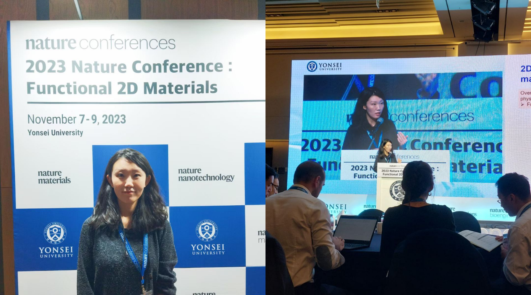 Dr Tian presenting her research at 2023 Nature Conference: Functional 2D Materials
Beyond the Limits of Silicon
Virtually every modern digital device relies on semiconductors, the materials formed into microchips that control the flow of electricity.
For decades, one material has dominated them all: silicon. It is relatively cheap, reliable, and one of the most abundant materials on Earth, refined from ordinary sand.
Nearly every computer, phone, and appliance ever made has been built on it.
Silicon is now reaching its limits. As devices grow smaller and demand more power, it struggles to keep up.
It runs hotter and loses more energy, which is why laptops warm up and chargers feel hot to the touch.
Why Gallium Nitride Matters
Researchers have been searching for a material that can run cooler and handle more power than silicon.
Gallium nitride, known as GaN, has emerged as one of the most promising candidates, and it is the material Dr Tian examines in this study.
It can withstand higher voltages, switch faster, and run more efficiently than silicon, which means less wasted energy and less heat.
GaN is already common in everyday technology such as electric vehicles and small, fast phone chargers, delivering more power while staying cool.
Beyond consumer electronics, GaN is increasingly being adopted in data centres, power grids and high-frequency 5G and emerging 6G communications, where its ability to operate efficiently under extreme conditions offers significant advantages over silicon (CSIS, 2024).
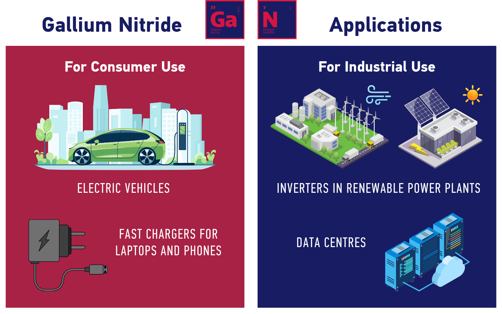 Figure 1: Infographic of GaN applications
Why Hasn't Gallium Nitride Replaced Silicon?
Given these advantages, a natural question is why GaN has not replaced silicon altogether.
The answer lies largely in manufacturing. Silicon benefits from decades of investment, which makes it inexpensive to produce at massive scale.
Unlike silicon, GaN does not occur naturally and must be grown using synthetic crystal techniques, which makes it scarcer and more expensive.
Large-scale production is still in its early days, with much of the cost driven by advanced processing equipment.
As a result, GaN is currently used mainly in specialised applications, while silicon remains the material behind mainstream electronics.
What Changes at the Atomic Scale
This is where Dr Tian Yujia's research comes in. Her study focuses on 2D GaN, an ultrathin form of GaN just a single atom thick.
Researchers have developed ways to grow gallium nitride as 2D sheets in the lab.
Using modern nanotechnology such as electron irradiation, they can even manipulate individual atoms to control the material's tiny imperfections with remarkable precision.
Reducing a material from a three-dimensional structure to a single atomic layer can change how it behaves. Dr Tian set out to measure exactly how much this would affect GaN.
The results revealed that ultrathin GaN needed an electric field around 30 times stronger than bulk GaN to trigger a change in its electronic behaviour. Both forms have the same chemical composition and differ only in thickness and structure.
"It highlights how profoundly quantum confinement can redefine material properties," Dr Tian reflects.
The finding suggests that ultrathin GaN could stay reliable under the high voltage conditions found in electric-vehicle chargers and power grids.
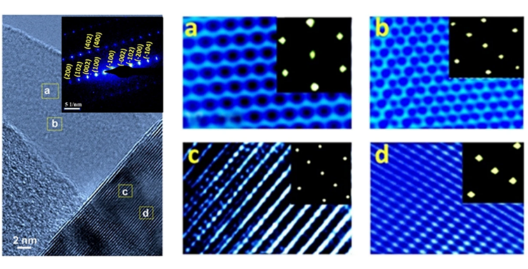 Figure 2: High-Resolution Transmission Electron Microscopy (HRTEM) image of chemically synthesized 2D GaN sheets obtained at different locations (a–d). Reproduced from Sahu et al. (2023).
Making a Simulation as Realistic as Possible
Most studies test materials one condition at a time, under near-perfect settings. A working device faces defects, strain and electric fields simultaneously.
Dr Tian's aim was to move beyond these idealised models and study 2D GaN as it would behave in the real world.
Modelling these conditions together reveals interactions that would otherwise be missed.
The simulations showed that these conditions can reinforce one another. Certain defects altered the material's electronic behaviour, while strain made those defects easier to form and could trigger those changes under weaker electric fields.
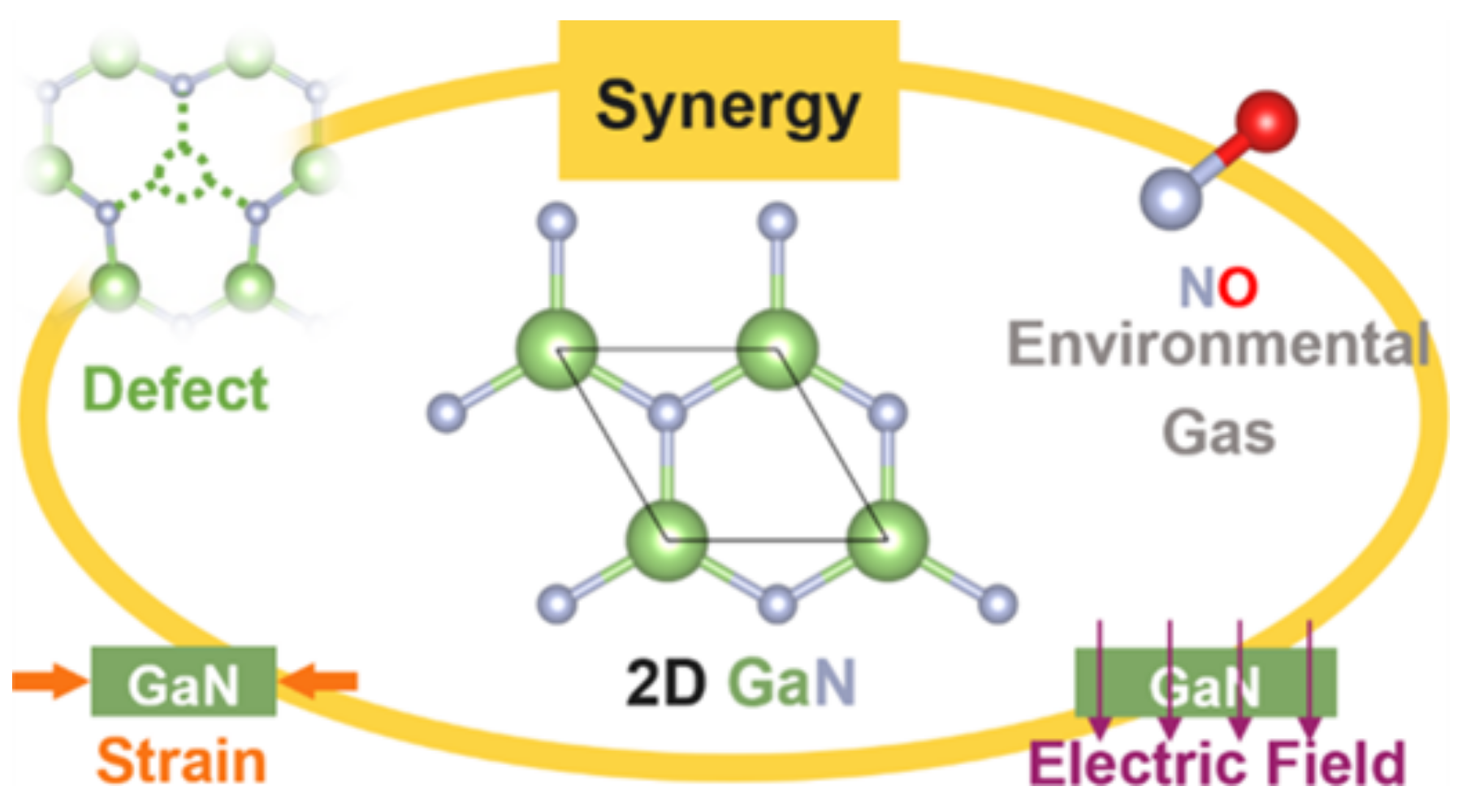 Figure 3: An overview of Dr Tian's study of 2D GaN.
Leveraging Defects in Design
Defects are usually seen as flaws to be removed. Dr Tian's finding overturns conventional thinking, showing that defects do not always harm performance.
Under strong electric fields, certain defects could improve the material's electronic stability. This challenges the long-held goal of eliminating them entirely.
Rather than trying to remove every defect, which is increasingly difficult and costly to do at the atomic scale, Dr Tian takes the opposite approach, explaining that "we can purposely introduce and engineer defects to unlock beneficial functionalities."
Engineering defects is more precise than it sounds. Dr Tian compares the atom-thin sheet of GaN to a microscopic chain-link fence. Firing a finely tuned beam of electrons at it can knock out a single atom, leaving behind a tiny gap, or defect, with a high degree of control.
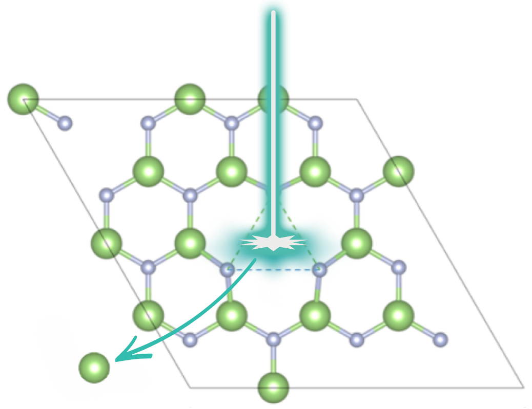 Figure 4: Simplified illustration of electron irradiation for defect engineering of 2D GaN
By adjusting the beam's energy, researchers can even choose whether to remove a nitrogen atom or a gallium one.
This ability to design defects matters for manufacturing. Defects are inevitable when making a material at this scale, so building with them is more practical than trying to eliminate them.
It could also make production more forgiving. When production lines become more tolerant of defects in 2D GaN, this could lower the number of chips rejected and reduce manufacturing costs.
Dr Tian also found that applying controlled compressive strain, essentially squeezing the material, allows the material to switch states at lower voltages, potentially enabling more energy-efficient electronic devices.
This matters because manufacturers could then use existing industrial strain-engineering techniques, rather than building complex, high-voltage nanoscale architectures.
These findings point towards defect-tolerant electronics that perform reliably under demanding conditions, and that are more practical to produce.
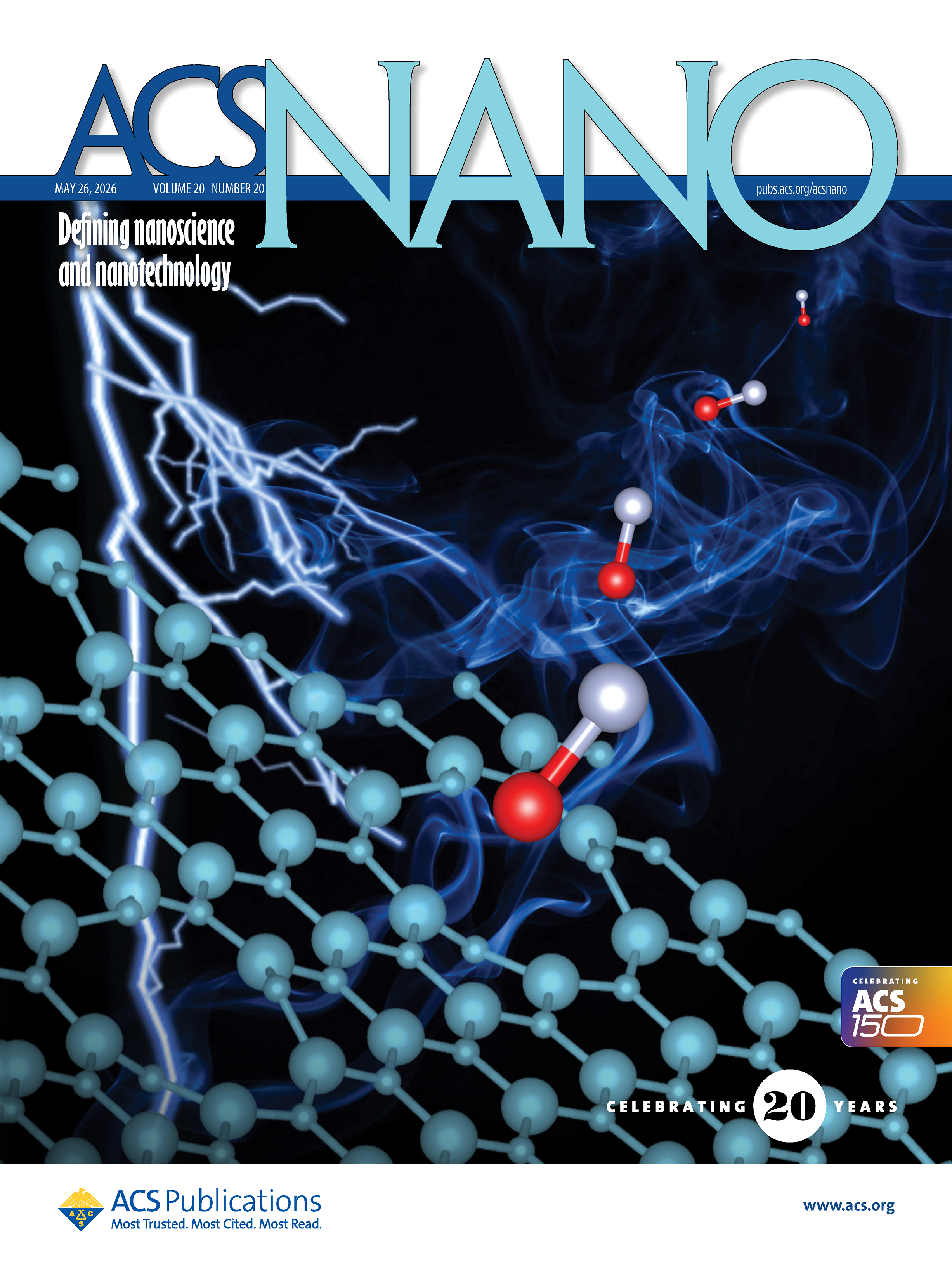 Dr Tian's work featured on the cover of ACS Nano (vol. 20, May 2026), showing a defective GaN monolayer sensing and capturing toxic gases under an electric field, represented by lightning.
Bridging Theory and Application
Having established these findings, the research is now ready for the next stage: testing the predictions in a physical laboratory.
From there, the research scope can widen to see how 2D GaN behaves across more conditions, including changes in temperature and the presence of magnetic fields.
Mapping how these factors interact will reveal where the material performs well and where its limits lie. These findings provide a blueprint for developing this atom-thin material into practical devices.
Dr Tian sees the path to mass production running through the industry's existing infrastructure.
Combining 2D GaN's structural advantages with emerging methods that bring GaN onto established silicon manufacturing lines could make large-scale production commercially viable.
Inspiring the Next Generation
Dr Tian is a recipient of the Women in Engineering, Science and Technology (WiEST) Development Grant 2025, which covers technical conferences and professional development courses for women early in their research careers.
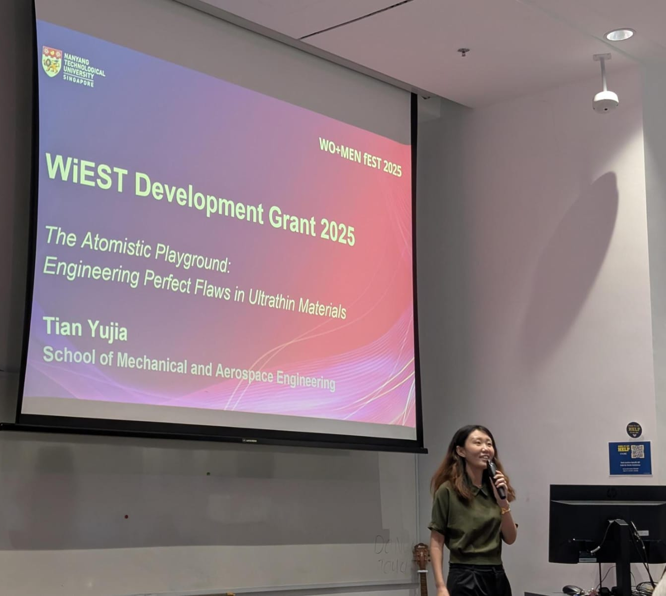 Dr Tian presenting her research at WO+MEN fEST 2025
“Supporting greater representation in STEM goes beyond balancing numbers. It is about cultivating diverse perspectives to solve complex technical challenges,” she says.
Having benefited from seeing female role models flourish in the field, she hopes to use her own research journey to become that guiding figure for others, encouraging junior researchers and students as they carve out their own paths in STEM.
.webp?sfvrsn=9ec5ca47_5 "SWE at NTU REsheARCH showcase") Dr Tian (second row, fourth from left) at REsheARCH Showcase 2026, organised by Society of Women Engineers at NTU.
Dr Tian (second row, fourth from left) at REsheARCH Showcase 2026, organised by Society of Women Engineers at NTU.
About Dr Tian YujiaDr Tian Yujia graduated from NTU's School of Mechanical and Aerospace Engineering (MAE) with a Bachelor of Engineering in Aerospace Engineering under the CN Yang Scholars Programme. She continued her academic journey at NTU MAE by pursuing a PhD with Professor Zhou Kun. As part of the Singapore Economic Development Board Industrial Postgraduate Programme, she collaborated with Infineon Technologies Asia Pacific Pte Ltd, where her research bridged first-principles modelling with real-world semiconductor applications. Dr Tian took on the role of research fellow at NTU MAE, specialising in two-dimensional semiconductors and heterostructures. Her research focuses on first-principles studies of their structural and electronic properties. In June 2026, she joined the Department of Materials Science and Engineering at the National University of Singapore as a Research Fellow. |  |
References
Tian, Y., Kripalani, D. R., Xue, M., & Zhou, K. (2026). Defect engineering of ultrathin gallium nitride via electric fields for advanced electronic, magnetic, and gas sensing applications. ACS Nano, 20(20), 14378–14391. https://doi.org/10.1021/acsnano.5c15014
Center for Strategic and International Studies. (2024). Gallium Nitride: A Strategic Opportunity for the Semiconductor Industry. https://www.csis.org/analysis/gallium-nitride-strategic-opportunity-semiconductor-industry
Sahu, T.K., Sahu, S.P., Hembram, K.P.S.S. et al. Free-standing 2D gallium nitride for electronic, excitonic, spintronic, piezoelectric, thermoplastic, and 6G wireless communication applications. NPG Asia Mater 15, 49 (2023). https://doi.org/10.1038/s41427-023-00497-6
By Regine Ng and Karen Chai, NTU MAE Communications
.tmb-listing.png?sfvrsn=892cad8a_1)