ZEISS Crossbeam 540
FACTS ABN B4
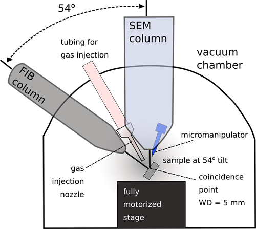
A focused ion beam (FIB) built on a FESEM platform for site-specific analysis, cross-sectioning, deposition and removal of materials and TEM lamella preparation.
Resolution : 0.9 nm @ 15kV (SEM) & 3 nm (FIB)
Accelerating Voltage: 0.1kV to 30 kV
FIB probe current: up to 40 nA
Attachments:
- In-lens Secondary electron detector & Backscattered (EsB) electron detector
- Secondary Electron and Secondary Ion imaging detector (SESI)
- Annular Scanning Transmission Electron Microscopy (STEM) detector
- Omniprobe manipulator
- Pt & C gas injection systems
- Energy Dispersive X-ray (EDS)
Samples for FIB operation should be restricted to dimensions of not larger than 10 mm x 10 mm x 5 mm (thickness). If not electrically conductive, they should be conductively coated to minimize sample drift during operation.
-
Cross-sectioning (cut flat section for looking into the material)
- Rapid and site-specific TEM lamella preparation (cut a thin lamella at specific site for TEM)
-
Nanopatterning (i.e. deposition or milling of complex patterns/features)
-
Creating electronic circuit
-
3D tomography (cut and view the external and internal structures of a specimen in 3D space)


