


/enri-thumbnails/careeropportunities1f0caf1c-a12d-479c-be7c-3c04e085c617.tmb-mega-menu.jpg?Culture=en&sfvrsn=d7261e3b_1)

/cradle-thumbnails/research-capabilities1516d0ba63aa44f0b4ee77a8c05263b2.tmb-mega-menu.jpg?Culture=en&sfvrsn=1bc94f8_1)

7e6fdc03-9018-4d08-9a98-8a21acbc37ba.tmb-mega-menu.jpg?Culture=en&sfvrsn=7deaf618_1)


Research Areas
Smoothening of Scalloped DRIE Trench Walls
Daniel Poenar
Deep reactive ion etch (DRIE) is often used for etching high aspect ratio trenches in silicon with vertical walls. However, the resulting scalloping of the trench walls can adversely influence subsequent process steps or the electrical behaviour of devices that use these trenches. We have successfully developed a simple planarization method employing successive thermal oxidation-oxide stripping steps which reduced the average scallop roughness of the etched trench walls by 80%, which is quite remarkable compared to other reported results and which also used high temperature annealing. The only extremely larger reported (96% reduction of peak-to-valley roughness) used FIB, hence is impractical and inapplicable for mass production. In contrast, our process is simple, practical, controllable, and easily adaptable for other initial roughness values. The smoothened trenches obtained with our process were easily filled with electroplated copper to act as turns of an on-chip copper inductor.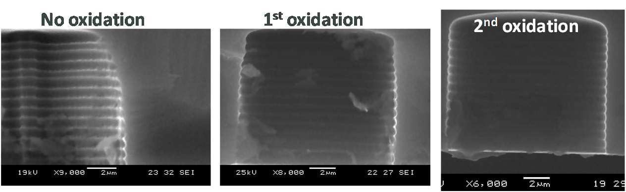
Fig. (a) SEM images of scallops with each oxidation showing smoothening after each step
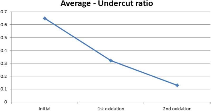
(b) Average values of the DRIE etched trench’s lateral wall scalloping undercut ratio, defined as the ratio (Average scallop depth)/(Average scallop pitch).
High Mobility Semiconductor Channel and High k Gate Dielectric Stacks
T.K.S. Wong [Email]
This project is a collaboration with IMRE. The objective is to realize metal gate high k dielectric gate stacks on high mobility compound semiconductors that are grown by MOCVD on Ge substrates. Zn doped GaAs epilayer was grown at 620oC using Ge(001) substrates with a 6o miscut using organometallic sources. Although Ge is nearly lattice matched to GaAs, anitphase defects were observed and resulted in surface roughness of ~5nm. High k dielectrics were deposited using atomic layer deposition. Thus far, two dielectrics, TiO2 and Al2O3 had been deposited at 200oC. The metal gate was deposited by magnetron sputtering. The two interfaces of the prepared samples were characterized by atomic force microscopy, secondary ion mass spectrometry and CV and IV characterization. Results showed that there is interdiffusion of Ge into GaAs and there is hysteresis in the CV curves due to the wider bandgap of the GaAs. This work was first presented in the MRS spring symposium in 2010 and was an invited paper in the 2011 IEEE International conference on nanoelectronics.
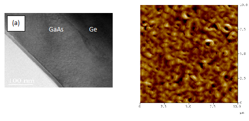
Fig. (a) Cross sectional TEM of GaAs on Ge; (b) topographic AFM image of Zn doped GaAs.
Mid-Infrared Polarization Splitter and Rotator on Silicon
Wang Hong
A mid-infrared silicon polarization splitter and rotator (PSR) is designed. The partially etched structure makes the device compatible with the metal back-end of line process. By using the grating-assisted coupler, the device is no longer limited by the precise control of the coupling length and strength, which is required for its counterparts based on directional couplers. The PSR can work over a wide spectral range of 50 nm around the wavelength of 2.5 µm with the typical TE-to-TM polarization conversion efficiency of 96.83%, conversion loss of -0.97 dB and polarization crosstalk of -21.48 dB. A fabrication tolerance larger than 45 nm has been achieved.
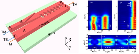
T. Hu, M. S. Rouifed, H. Qiu, X. Guo, C. G. Littlejohns, C. Liu, and H. Wang, IEEE PHOTONICS TECHNOLOGY LETTERS, 2011: A Polarization Splitter and Rotator Based on a Partially Etched Grating-Assisted Coupler
Disruptive Air-gapped Microcoaxial Transmission Line Technology
Wang Hong
The disruptive air-gapped microcoaxial transmission line (MCTL) technology utilized a multilayer Cu damascene process is developed for Si-based microwave applications. It has a low thermal budget and full compatibility with complementary metal-oxide-semiconductor (CMOS) back-end-of-line (BEOL) process. The MCTL technology shows superior performance for ultra-low loss (< 0.02 dB/mm), low and constant effective permittivity (~1.02), and perfect signal isolation (> 60 dB) in the frequency range 0.1 to 40 GHz. Conventional microwave components can be converted to fully 3D components integrated with CMOS circuit on Si substrate, with more superior performance. Demonstrated works include true-time-delay (TTD) lines, cavity resonators and filters, power combiner/splitter, branch-line couplers, and rat-race hybrids. The designed and measured results show excellent matches between, proving the technology’s usefulness for practical applications.
 Y. Tian, K. Lee, and H. Wang, IEEE Microwave and Wireless Components Letters 2014: A 390 ps on-wafer true-time-delay line developed by a novel micro-coax technology.
Y. Tian, Q. Meng, K. Lee, and H. Wang, IEEE Microwave and Wireless Components Letters 2015: Low-loss microcoax-to-CPW transition for air-gapped microcoaxial passives.
Y. Tian, N. Li, K. Lee, X. Li, and H Wang, IEEE Transactions on Components, Packaging and Manufacturing Technology 2016: Right-angled microcoaxial bends for Si-based RF/microwave integrated circuits.
Y. Tian, H. Wang, Z. Liu, Q. Meng, and K. Lee, IEEE Microwave and Wireless Components Letters, 2016: Low loss microcoaxial rat-race hybrid for Si-based microwave integrated circuits.
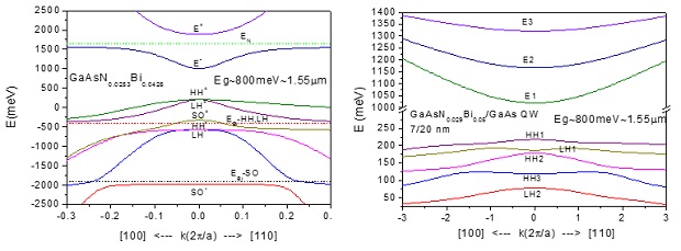
The band structures GaAsNBi and GaAsNBi/GaAs quantum well are investigated by using the 16-band k•p method. When N composition is 0.58 of Bi composition, GaAsNBi is lattice matched to GaAs.
Fan Weijun
Compressive strained GaAsNBi, lattice matched GaAsNBi and GaAsNBi/GaAs QW band structures are calculated and obtained for the fundamental transition at 1.55um.
Loeblein M, Bolker A, Tsang SH, Atar N, Uzan-Saguy C, Verker R, et al. 3D Graphene-Infused Polyimide with Enhanced Electrothermal Performance for Long-Term Flexible Space Applications. Small. 2015;11(48):6425-34
Edwin Teo Hang Thong
Next-generation thermal control and shielding blankets for space vehicles are demonstrated by using 3D graphene-reinforced polyimide hybrids. The hybrid is space qualified and achieves outstanding thermal and electrical characteristics, exceeding nominal values by 1033% and 10 orders of magnitude, respectively. Its long-term stability in space is extensively tested through ageing and mechanical deformation studies, in a ground-based simulated space environment. This hybrid material is shown to provide excellent electrostatic discharge shielding protection with long-term stability in harsh environments. This is a collabration work by EEE-NTU, CINTRA and Soreq nuclear research center, Isreal.
This work is featured in the front cover of Small. 11, Vol (48), 2015
95325f2e-efe0-4313-bc99-e154b2d4e4d2.jpg?Status=Master&sfvrsn=ce74529_3)
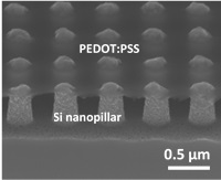
High Efficiency Si/PEDOT:PSS Hybrid Solar Cell based on Periodic Nanopillars
Rusli
The emerging hybrid Si/PEDOT:PSS solar cells have been actively explored in the recent years. In this study we present the hybrid solar cells based on periodic Si nanopillars with different pitches formed by plasma etching. We propose a simple surface treatment method using a mixed HF, acetic and HNO3 solution (HAN) solution, which can dissolve the surface damage layer arising from the dry etching process, and also increase the surface roughness of the silicon nanopillars. Benefitting from the optimization of the surface quality and efficient light absorption of the Si nanopillars, a highest power conversion efficiency of 11.8 % has been achieved for the hybrid cell with a pitch of 600 nm and nanopillars height of 600 nm. Our work also paves the way for the study of dimensional effect and optimization of the hybrid solar cell based on the periodic Si nanopillars.
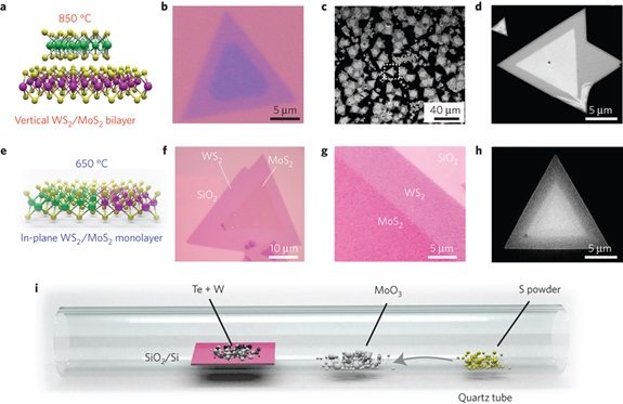
Vertical and In-plane Heterostructures from WS2/MoS2 Monolayers
Tay Beng Kang
We report a one-step growth for the high-quality vertically stacked and in-plane interconnected heterostructures of WS2/MoS2 via control of the growth temperature. Vertically stacked bilayers with WS2 epitaxially grown on top of the MoS2 monolayer are formed with preferred stacking order at high temperature. A strong interlayer excitonic transition is observed due to the type II band alignment and to the clean interface of these bilayers. Vapour growth at low temperature, on the other hand, leads to lateral epitaxy of WS2 on MoS2 edges, creating seamless in-plane heterostructures that generate strong localized photoluminescence enhancement and intrinsic p–n junctions.
(Prof Tay Beng Kang, Nature Materials, 2014, 13, 1135–1142)
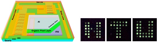
Carbon Nanotube Driver Circuit for Organic Light Emitting Diode Display
Zhang Qing
Jianping Zou, Kang Zhang, Jingqi Li, Yongbiao Zhao, Yilei Wang, Suresh Kumar Raman Pillai, Hilmi Volkan Demir, Xiaowei Sun, Mary B. Chan-Park and Qing Zhang, “Carbon Nanotube Driver Circuit for 6 × 6 Organic Light Emitting Diode Display”, Scientific Reports 5(2015)11755.
Single-walled carbon nanotube (SWNT) is a very promising material for flexible and transparent driver circuits for organic light emitting diode (OLED) displays due to its high carrier mobility, current carrying capacity, transparency, and flexibility. Chemical vapor deposition (CVD)-grown SWNT network thin film transistor (TFT) driver circuit has been successfully developed for static and dynamic OLED displays with 6 × 6 pixels. The high device mobility of ~ 45 cm2V-1s-1 and the high channel current on/off ratio of ~ 105 of the SWNT-TFTs fully guarantee the control capability to the OLED pixels.