Free electron nanophotonics
Extreme electron-photon interactions in nanomaterials
Rapid strides in nanofabrication, electron manipulation and photon waveshaping have opened vistas of new fundamental phenomena and potentially disruptive technologies. These range from portable sources of high-quality X-rays and gamma rays to highly efficient energy conversion techniques, with applications in medical imaging, security scanning, industrial inspection and next-generation computation.
Learn more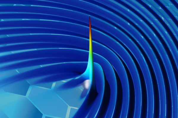

Exotic electromagnetic waveshaping
Maxwell's equations are over a hundred years old, but new electromagnetic phenomena continue to be discovered, unlocking revolutionary techniques in imaging, microscopy and materials processing. These phenomena include novel electromagnetic wavepackets exhibiting unprecedented physics and new ways of shaping light with nanomaterials.
Learn moreAdvanced electron manipulation with shaped laser pulses
Electron-based instrumentation -- ranging from desk-sized scanning electron microscopes to kilometers-long X-ray free electron lasers -- form a cornerstone of modern scientific progress and industrial development. The advent of ultrafast optics and nanomaterials promise more compact, versatile and cost-efficient methods of electron beam transport and control. These methods include high-gradient laser-driven electron acceleration and attosecond-scale electron pulse generation.
Learn more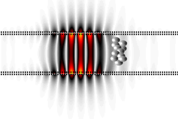
Straintronics for Revolutionizing Integrated Photonics
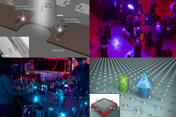
Our research group is dedicated to developing and applying innovative strain engineering techniques for discovering unprecedented optical properties in various materials. More specifically, we develop a new class of photonic devices including lasers and photodetectors for the realization of integrated optical and quantum computing technologies.
Learn moreGas mixture sensing with broadly tunable and long wavelength QCL.
As the spectra fingerprint region, Mid-Infrared provide fundamental ro-vibrational band absorption information. Quantum cascade laser, as an ideal coherent source in mid-infrared wavelength range, has drawn increasing attention in gas sensing area. However, to realize gas mixture monitoring requires broadly tunable laser source that cover the featured peaks of all compositions. Moreover, several VOCs, including benzene, xylene, and toluene, only have strong IR absorption at around 13~14 um, which is still quite challenging for QCL design. We then aim to develop high performance, broadband tuning, and long wavelength QCL source for gas sensing application. Afterwards, we integrate a tunable QCL source and a hollow core fiber as the gas cell in a compact sensing system. The AI algorithm, advanced extreme learning machine (ELM), is then introduced to realize quantitative spectra analysis.
Learn More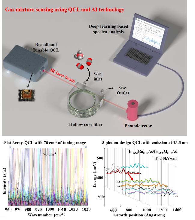
Mid-infrared photodetectors based on 2D materials
Graphene and other related two-dimensional materials exhibit diverse optical and electrical properties, which accommodate a large potential in optoelectronic applications such as photodetection. However, although much progress has been made, various challenges such as the absence of bandgap, low absorption and short carrier life-time, hinder their applications. Nano-patterning, graphene p-n junction and hybridization are employed to improve the performance of graphene based photodetector. Furthermore, other two-dimensional noble metal chalcogenides with proper defect engineering are also used in near-IR photodetections.

Graphene p-n junction photodetector
(a) schematic design and (b) mechanism of graphene p-n junction; (c) The electric characteristics as a function of gate bias of the intrinsic graphene FET; (d) Photocurrent measured in one period of modulation.

Hybrid graphene/Ti2O3 photodetector
We demonstrate a mid-infrared hybrid graphene photodetector enabled via coupling with a narrow bandgap semiconductor. The obtained photoresponsivity here is about two orders of magnitude higher than that of commercial mid-infrared photodetectors. The photoresponse is enhanced with increasing graphene layers, resulting from stronger dipole-dipole interactions and more efficient carrier separation in the hybrid structures with thicker graphene.

Hybrid graphene/C60 photodetector
All-carbon graphene nanoribbon-C60 hybrid nanostructure is demonstrated to achieve a high photoresponsivity of 0.4 A/W under mid-infrared laser illumination at room temperature. Such high performance is achieved through the high electron trapping efficiency of C60 film as deposited onto 10-nm-wide graphene nanoribbons.

Bilayer PtSe2 photodetector
Bilayer PtSe2 via proper defect engineering is explored as an effective room-temperature mid-infrared photodetector with high speed and responsivity. The narrow band gap nature of atomic layer of PtSe2 makes it suitable for mid-infrared photonic devices.
Mid-IR and Terahertz Science and Technologies
The mid-infrared (3-20 µm) and Terahertz (THz) (30-300 µm) regions remain as some of the least developed spectral regions, despite their proven important applications in chemical sensing, spectroscopy, material sciences, security screening, biomedical imaging, astronomy science, etc. However, a breakthrough is needed for the emerging mid-IR and THz technologies to develop high performance semiconductor-based lasers, modulators, and photo-detectors that are suitable for industry mass production.

Broadly Tunable Single-Mode QCLs

Integrated THz Graphene Modulator

Graphene Plasmonics

