
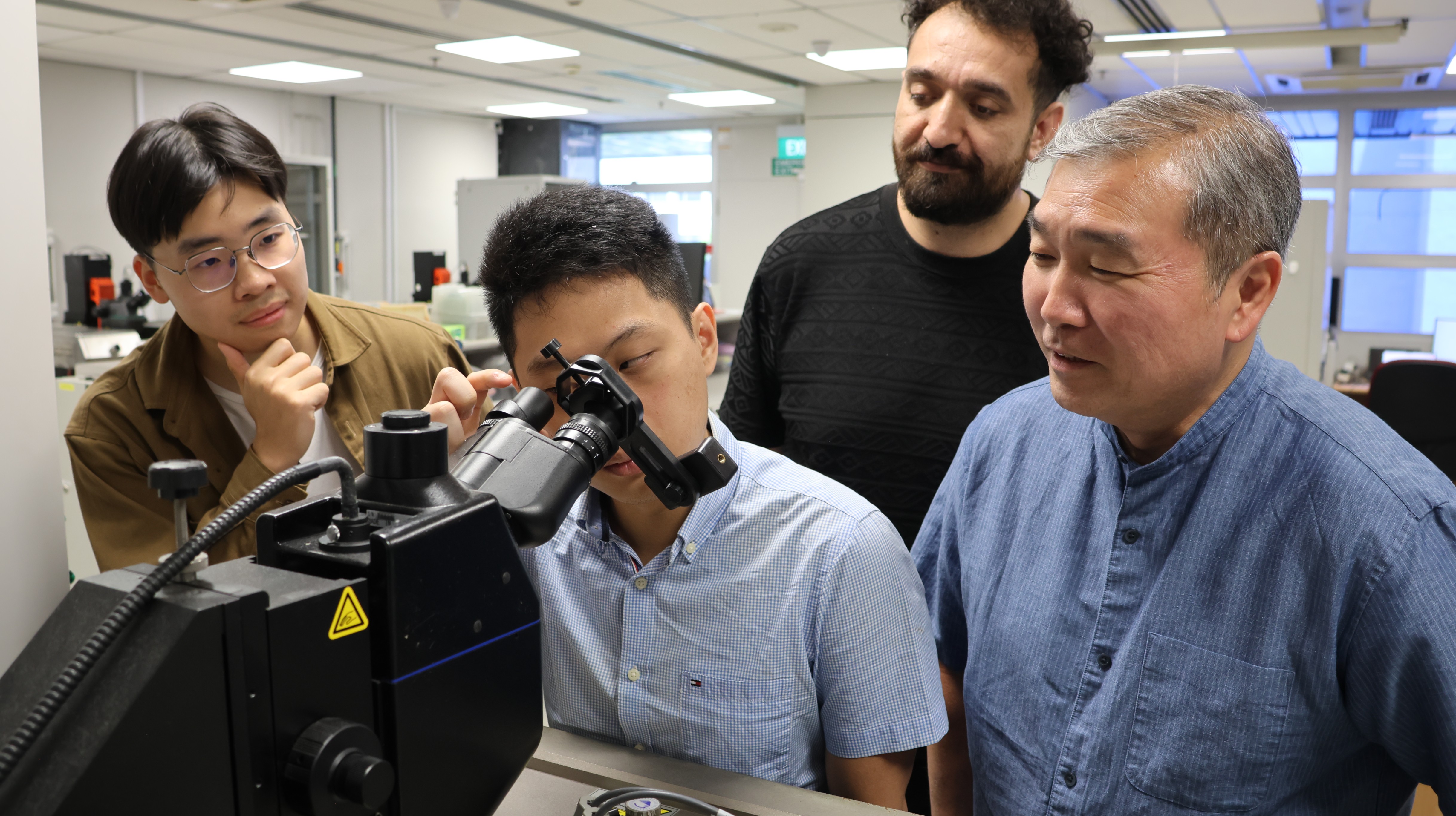
NTU Singapore researchers demonstrate a robust conductive-bridge memory prototype capable of nanosecond-speed, multi-bit storage at below one volt for more than 10 million operation cycles. This new technology could potentially advance the development of faster and more energy-efficient edge AI systems.
Artificial intelligence (AI) is rapidly moving from data centers into mobile phones, autonomous systems (robots, self-driving vehicles, drones, etc.), intelligent sensors and wearable devices. However, many edge devices still need to transfer AI models and data repeatedly between the processor and separate memory chips. This constant shuttling of data introduces delays and consumes most of the energy of AI compute.
Researchers from NTU Singapore have developed a new conductive-bridge random access memory or CBRAM that could help overcome this bottleneck by enabling much larger amounts of non-volatile memory to be integrated directly onto an AI processor.

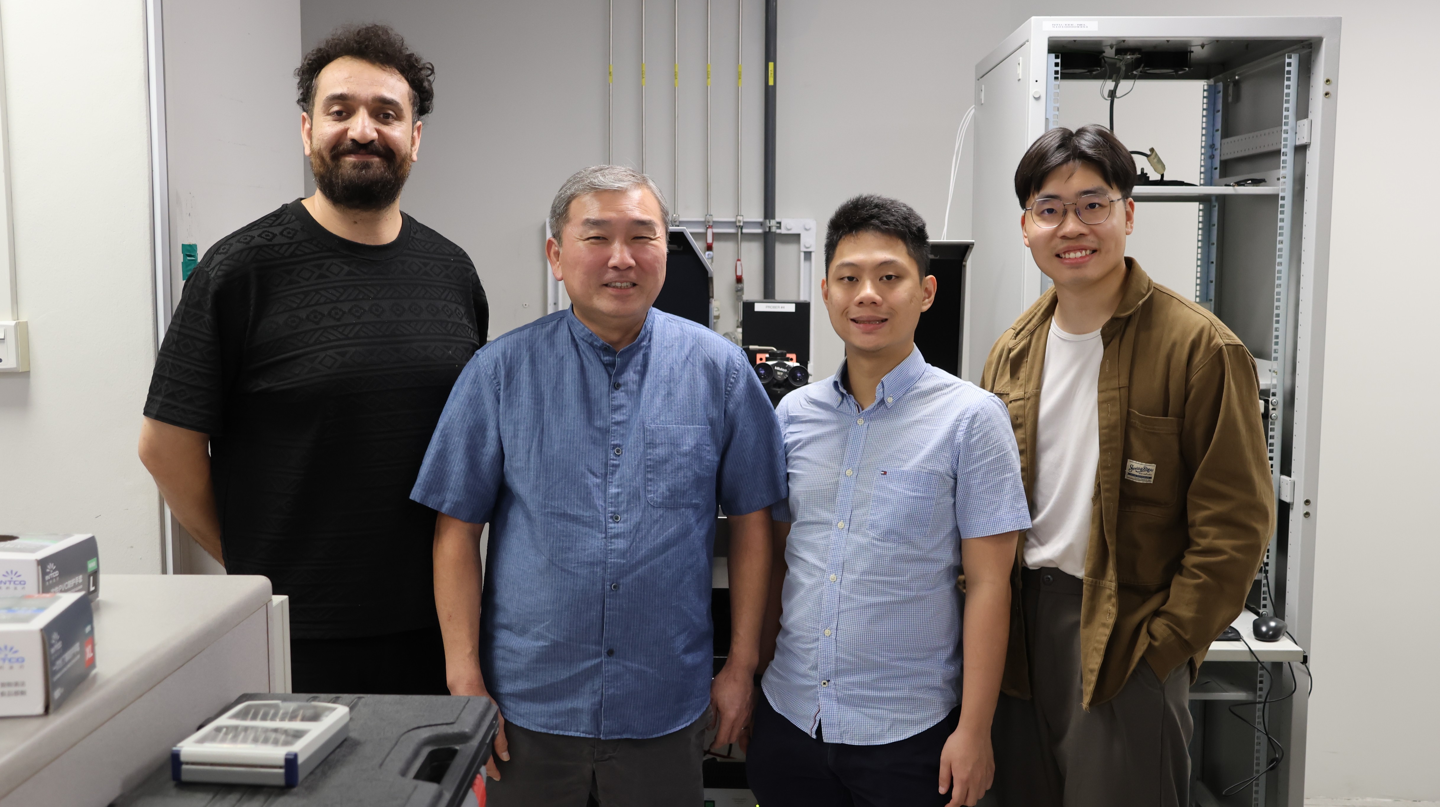
Led by Associate Professor Diing Shenp ANG from the School of Electrical and Electronic Engineering (EEE), the research team demonstrated that its CBRAM technology can operate at nanosecond speeds, at voltages below one volt and store multiple bits in one cell with reliable switching performance for more than 10 million program/erase cycles. Achieving these characteristics simultaneously over millions of operation cycles is an important step towards practical, high-density storage memory that can be manufactured alongside advanced computing circuits.
The team’s longer-term goal is to develop CBRAM into a gigabit-class on-chip memory capable of storing an entire AI model close to or within the processor. Keeping AI models on chip greatly reduces the need to retrieve the information from external memory, allowing edge devices to make decisions with lower latency and substantially less energy.
Such an approach could support a new generation of compact and responsive AI systems, including autonomous robots, drones, smart cameras, medical devices, industrial sensors, etc. It could also enable always-on intelligence with near-instantaneous wake-up, while reducing reliance on continuous cloud connectivity. Limiting the amount of sensitive data transmitted to remote servers and processing it locally also improves privacy.
CBRAM is a form of resistive random access memory or ReRAM in which data are stored by the controlled formation and removal of an extremely small conductive bridge inside the memory cell. Its simple device structure and potential for vertical integration allow memory cells to be tightly packed in a small chip area, paving a way for the realization of high-density embedded memory.
In the longer term, the combination of high speed, sub-1 V operating voltage, non-volatility, multi-bit storage capability and high integration density may position the technology as a candidate for a unified memory architecture. Such a memory could potentially combine the advantages of today’s DRAM and Flash, although substantial development and large-scale validation are still required before it can replace these established memories.
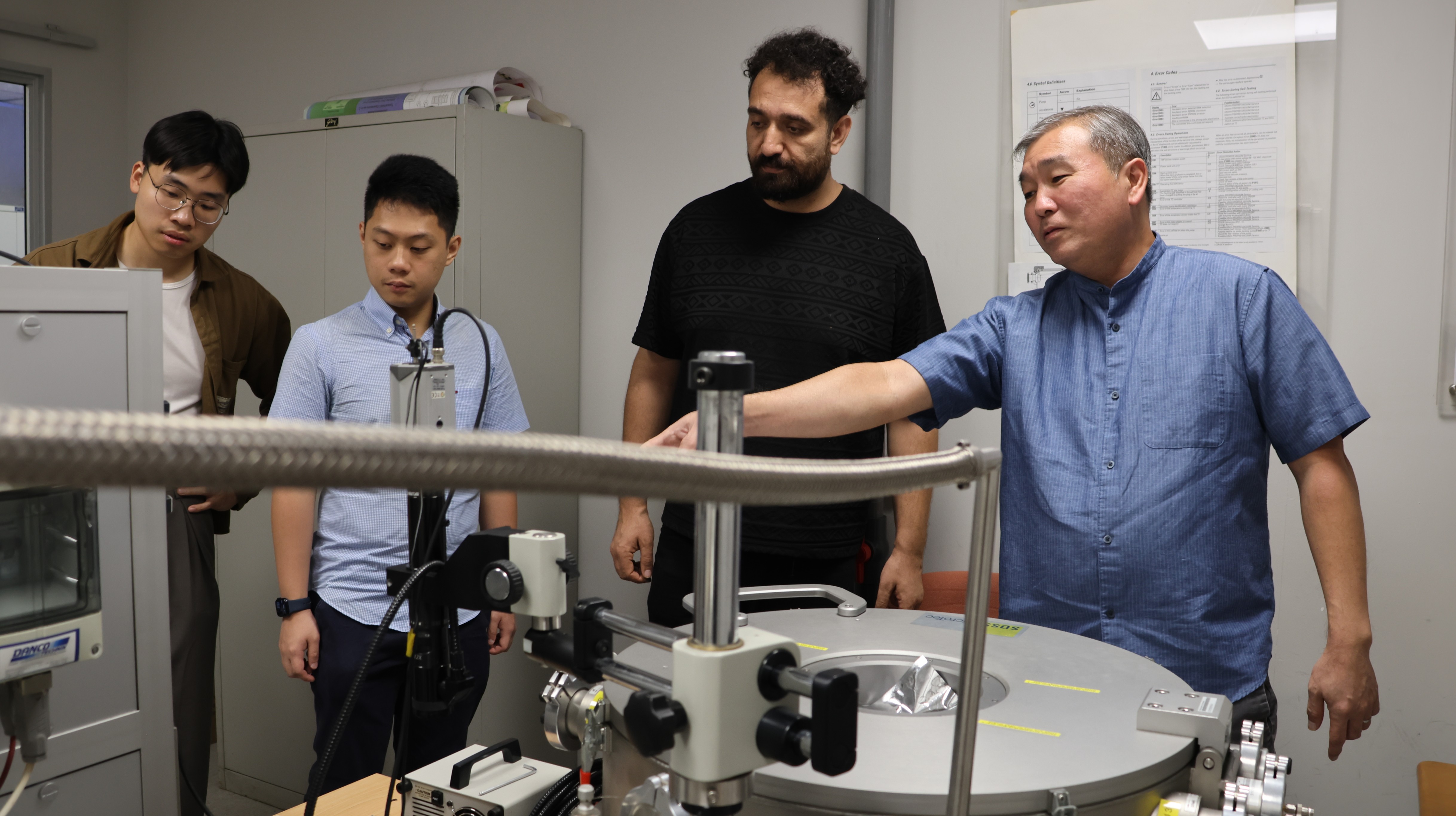
“For edge AI to become truly intelligent and energy-efficient, we need to eliminate the constant movement of information between the processor and external memory. Our approach to overcoming this challenge is to develop a gigabit-class memory that can be integrated directly on an AI chip, so that the complete AI model can remain close to where computation takes place.
A major challenge to this end has been achieving a logic-compatible memory technology with fast nanosecond-scale switching, sub-1 V operating voltage, multiple bit storage and reliable operation all at the same time. Our results show that these requirements can be brought together in a single conductive-bridge memory technology. Under these stringent voltage and timing conditions, our current prototype also exhibits a robust 10-year memory retention at around 85 °C. Our work represents an important step towards dense, low-power on-chip memory for future edge AI systems.
We hope to work with industry partners to scale the technology from prototype arrays toward practical memory chips for real-world AI applications.” - Associate Professor Diing Shenp ANG
The team will present its findings at the upcoming International Conference on Solid State Devices and Materials (SSDM) in Japan. Designed to bridge cutting-edge research with market realities, SSDM serves as a premier forum for industry executives and academic pioneers to collaborate on the future of semiconductor and memory innovations.